Moore’s Law has shaped the world we live in today. As smaller, cheaper, more powerful microchips continue to transform the global economy, a little-known company in the Netherlands has emerged as a vital linchpin in the semiconductor industry.
A Dutch commuter town might not be the first place you would expect to find a company operating at the frontier of technology and innovation, but Veldhoven, some 15 minutes south east of Eindhoven, is home to a company often dubbed “the most important tech company you’ve never heard of”. For once, such a lofty claim is not hyperbole: ASML is certainly no household name, but without its ground-breaking work much of the technology we take for granted today would not be possible.
Since its founding in 1984, ASML has been integral to the semiconductor ecosystem and a key enabler of Moore’s Law, the empirical observation made by Gordon Moore, the co-founder of Intel, that states that the number of transistors in a given area of a semiconductor will double every two years, exponentially increasing the computing power while decreasing the cost of the chip. The resultant smaller, cheaper, more powerful chips are the keystones of our current technology revolution, transforming every corner of the global economy, from communication and entertainment to healthcare and industrial manufacturing.
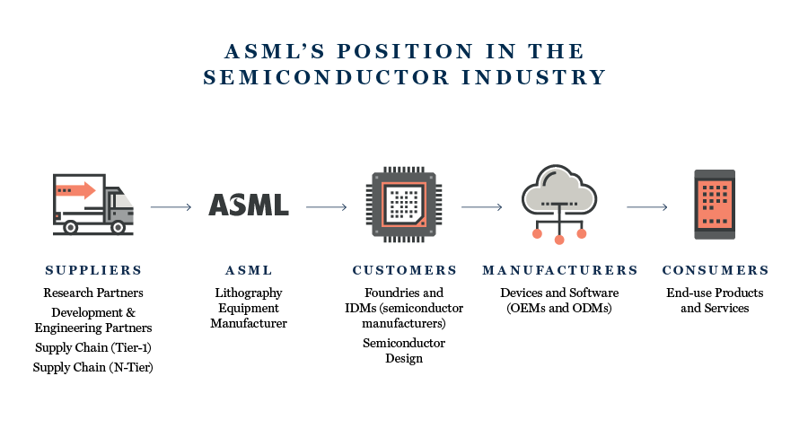
Spun out of Dutch electronics giant Philips in 1995, ASML has grown to become the dominant player in one of the critical steps in the production of semiconductors – lithography
Spun out of Dutch electronics giant Philips in 1995, ASML has grown to become the dominant player in one of the critical steps in the production of semiconductors – lithography. The process of using light to trace integrated circuits onto silicon wafers, it is lithography that determines how small the features on a chip can be, and how densely manufacturers can pack transistors together. Progress in lithography is predicated on ever shorter light wavelengths – the shorter the wavelength, the smaller the features that can be printed in a lithography process. Today, the most advanced form of lithography technology is ‘extreme ultraviolet’ (EUV). Occurring naturally in outer space, EUV light has a wavelength 14 times shorter than deep ultraviolet (DUV) light, the previously most advanced technology used in lithography. The result of huge investment and decades of R&D, EUV lithography has been credited with “saving” Moore’s Law and ensuring it will extend well into this next decade and potentially beyond.
To date, only one company in the world has mastered EUV lithography: ASML. Long the leading player in DUV with a market share that dwarves those of its two main competitors Nikon and Canon, for more than two decades the company worked painstakingly to develop a commercially viable EUV system. The importance of the prospective technology to the semiconductor industry was evidenced in 2012 by large-scale investment in the development process from TSMC, Samsung and Intel. To accelerate the development of key technologies, ASML also launched a series of astute acquisitions, including Cymer (lithography light sources) in 2012 and Hermes Microvision (e-beam metrology) in 2016, while at the same time working collaboratively with two German companies, Zeiss and Trumpf, to develop the necessary optical instruments and lasers. Finally, having overcome considerable scientific and technological challenges, ASML launched the TWINSCAN NXE:3400, a system that one technology insider has labelled “the most complicated machine humans have built”.
Even a cursory explanation of what occurs inside these machines gives a sense of the complexity involved
Even a cursory explanation of what occurs inside these machines gives a sense of the complexity involved. Every second, 50,000 droplets of molten tin are hit by two lasers. The first laser flattens the droplet, while the second vaporizes it to create a plasma that projects light onto a blueprint of the pattern that will be printed on the chip via a highly complex system of exceptionally precise mirrors (the mirrors are so smooth that if expanded to the size of Germany they would not have a bump higher than a millimetre). The pattern, now encoded in the light, is then printed onto a silicon wafer. Pattern is laid upon pattern hundreds of times over before the semiconductor is complete. Comprising more than 100,000 components and weighing 180 tonnes (three Boeing 747s are required for shipment), each machine will cost the purchaser up to US$200 million – complexity on this scale does not come cheap.
It is through this combination of technical proficiency, vertical integration, and collaboration, that ASML has established its de facto monopoly in EUV, which, given the high barriers to entry created by its technical complexity and the requirement for large-scale investment, is unlikely to face challenge for the foreseeable future. While demand is still at an early stage (most semiconductors continue to be manufactured using DUV technology), it is now well established and growing fast. In 2020, ASML made €4.5 billion from the sale of 31 EUV machines.1 In the second quarter of 2023 alone, the company took €4.5 billion in net bookings.2
Demand will continue to grow. A significant portion of the huge capital expenditure plans of Samsung, TSMC and Intel will be directed towards upping their EUV capacity.
Driving this demand is one of the global economy’s most compelling long-term growth trends: the expansion of the world’s digital infrastructure and the increasing prevalence of semiconductors across sectors
Driving this demand is one of the global economy’s most compelling long-term growth trends: the expansion of the world’s digital infrastructure and the increasing prevalence of semiconductors across sectors. By 2029, the value of the global semiconductor market is projected to reach US$1,381 billion, up from US$573 billion in 2022, a compound annual growth rate of 12.2%.3 Few, if any, industries are untouched by the digital revolution, and the emerging trends of recent years, artificial intelligence, automation, 5G, Big Data and the Internet of Things, have an insatiable appetite for faster and more powerful chips. Meeting this demand will be impossible without EUV and ASML. As Moore’s Law continues to change our world in unforeseen ways, “the most important tech company you’ve never heard of” will be central to the transformation.
Sources:
1 ASML 2020 Financial Results
2 ASML Q2 2023 Financial Results
3 Fortune Business Insights https://www.fortunebusinessinsights.com/semiconductor-market-102365
Important Information
This article is provided for general information only and should not be construed as investment advice or a recommendation. This information does not represent and must not be construed as an offer or a solicitation of an offer to buy or sell securities, commodities and/or any other financial instruments or products. This document may not be used for the purpose of an offer or solicitation in any jurisdiction or in any circumstances in which such an offer or solicitation is unlawful or not authorised.
Stock Examples
The information provided in this article relating to stock examples should not be considered a recommendation to buy or sell any particular security. Any examples discussed are given in the context of the theme being explored.